|
|
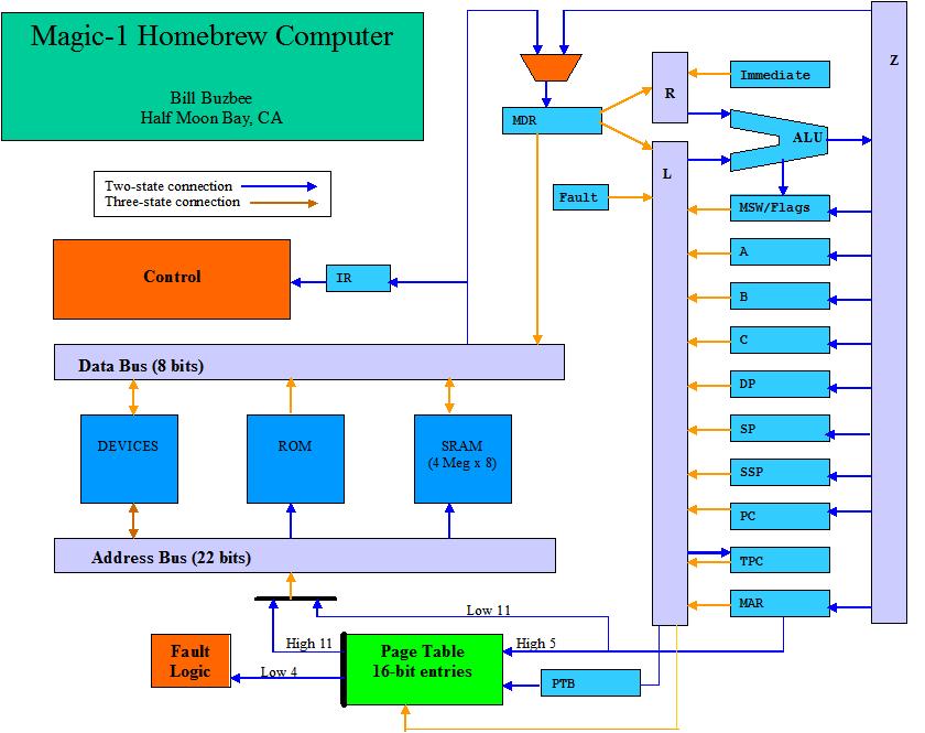
OverviewHere's a sketch of the basic block diagram:
Index
Hardware designSchematics are here. Registers & ALUsIn most of the similar projects that I've seen, registers have been built by using TTL register files or simply SRAM. The register file devices are somewhat exotic and difficult to find, and don't have as much flexibility as I'd like. Using SRAM just didn't seem esthetically right to me, so I ended up designing with D flip-flops. For situations which the register has a single output to one of the internal busses, I use a pair of 74374 octal D flip-flops with 3-state output. Examples of this are A, B, C, DP and SSP. In cases in which the output of the register has only one non-bus destination, I use 74273 octal D flip-flops with 2-state output. Examples of this are the Instruction Register (IR) and the Page Table Base (PTB). There are also a few cases in which I need both 2-state and 3-state outputs. Here I also use 74273s for the basic register, and then provide a 3-state connection to the bus with a pair of 74241 octal 3-state non-inverting buffers. Examples of this are MAR, SP and PC. For the main integer unit ALU, I originally designed in four of the old 74181 4-bit ALU parts with 74182 lookahead carry generator. I later, though, moved to a variant of the '181 - the 74F381. It is pretty much the same, except that it reduces the number of functions provided to the 8 useful ones (allowing me to drive the ALU with fewer microcode bits). The final configuration is 3 74F381s, one 74F382 and the 74F182 lookahead carry generator. The 74F382 is used as the most significant nibble in the ALU. It is the same as the 74F381, except that instead of providing carry generation output, it produces an overflow signal. For left-shift functionality, I simply add the operand to itself. For right-shift, I'll have an alternate bus driver hanging off the ALU output with a hard-wired 1-bit shift to the right. There will be no direct rotate support - you'll have to do a bit-test first to detect the state of the "rotated" bit, do a normal shift and finally OR in the rotated bit. In addition to the alternate right-shift bus driver, there will also be an alternate bus driver for sign extension hanging off the ALU output. So, the ALU is going to be a bit messy, with three distinct 3-state output connections to the Z bus:
Internal BussesThere are 3 internal busses connecting the registers and ALUs. Two busses, L and R, correspond to the left and right operands of an aluop. The other bus, Z, is the output of the ALU. In order to avoid microcode mistakes from damaging the machine, it will be possible for only one entity to drive a bus at a time (with one exception, see note below). The operand busses will have a corresponding "Enable" field in the microcode which will feed into a field decoder , the output of which will drive the 3-state enables of the various devices hanging off that bus. If only the low byte of the Z bus is being driven by the ALU, then we automatically drive the high byte of the Z bus with a copy of bit 7 of the low byte. This provides the sign extend functionality. The possible drivers for the various busses follow. Note that MDR can drive either or both operand busses.
ClocksThere is one master clock, CLK_S which is generated on the front panel logic card and travels to the control card. There, it is combined with microcode bits to generate edge-sensitive signals and drive the microcode sequencer state machine. In essence, the second half of each clock cycle (starting with CLK_S going high) is devoted to generating control signals. The first half of the following cycle is devoted to marshalling data based on the control signals, which are clocked on the rising edge of the various edge-sensitive signals. In retrospect, this design was too simple. As a software guy, I had a tendency to think of the clock pulse causing everything to happen at the same time. In fact, propogation delays mean that the clock edge wave reaches different parts of the system at very different times. As a result, there are places in Magic-1 where I had to specifically select fast (74Fxx) vs slow (74LSxx) parts to sidestep timing issues. In general, this is not a good thing - and could have been avoided if I had a series of overlapping clocks to select from. MicrocodeIn other examples of homebuilt CPUs that I've seen, remarkably little microcode was necessary. This is largely the result of having fairly wide and regular instruction encodings. In this way, bit patterns within the instruction word itself can be used to generate the control signals (RISC-like). On the other extreme, you could use the instruction word simply as an index to the starting address of the corresponding microcode program used to carry it out and not use any portion of the instruction bits to assist control signal generation. What I've done is something close to the latter. Wherever convenient, I'm using instruction bits to assist signal generation, but primarily I'm using the instruction byte as a direct index into the microcode. My original plan had me using the 8-bit opcode as in index into a PROM of starting addresses in the main microcode store. However, that added a lookup latency in the control signal generation path, so I decided to just burn more PROM bits and have the opcode be a direct starting address. So, for microcode I'm using five 512x8-bit PROMs. The low half of the PROM will be devoted to the first microinstruction of each instruction. Each microinstruction contains a "next" field, which will route microexecution into an appropriate spot in the other half of the microcode store. Within the sequencer there is the ability to conditionally branch. I recently also allowed a 1-deep subroutine call/return mechanism, but decided to drop it when it became clear that I had lots of unused space in the microcode PROMs. Not especially elegant, but it certainly simplified the sequencer. Oh, there's also a special microinstruction for fetching, and lots of nasty logic dealing with faults and interrupts. Interrupts will be recognized at instruction boundaries. Faults will immediately suppress clocking of results and will transfer control to a fault microcode sequence at the beginning of the next T cycle. As far as the parts used, I'm going with 74s472's, which are expensive and hard to find. For this reason, I put together an EPROM daughter card to try things out before I burn the real PROMs. The daughter card uses fast 60ns 27C256 EPROMs and also provides a hex display to show the address of the next microinstruction. [Note: as of this writing, I'm still using the EPROM daughter card and am inclined to just keep using it permanently]. So far, the part of the M1 design that I'm most embarrassed about is the large amount of microcode I'm using. I can see how I could significantly reduce it (in particular, by factoring in T-state pulses to give particular bits different meaning during different T-states). However, given that I'm going to be hand-wiring every connection, I think it best to trade off microcode bits for reduced complexity. Here's the current state of the M1 Microcode. Microcode Sequencer
Fetch/Execute SequenceM1 features a single fetch/decode clock cycle, followed by 1 or more execute clock cycles. A lot goes on in the fetch cycle. First, note that we assume that the Memory Address Register (MAR) has been loaded with the next instruction address in T-1, and we require that all instructions set up PC for the next one. Following is a typical instruction fetch/decode/execute cycle, an immediate add of #32 to the accumulator, or "ADD.8 A,#32". To try to show the sequence of events, I'll tag the steps with [L] for low system clock, [R] for rising edge, [H] for high clock and [F] for falling system clock. Clock 0
Clock 1
Clock 2
|